


 Thomas Thiel, 09/02/95
Architecture of a single processor node
Each node of the MEMSY system is identically designed and consists of a
Motorola multiprocessor board MVME188 and additional hardware, some of
which were designed and implemented as part of the MEMSY project.
The figure below shows the logical structure of a node. (The parts in
green were specically designed and the parts in red are off-the-shelf
components.)
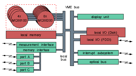
All components are assembled in one VME bus rack:
 From the left to the right you can see
The processor module comprises the system controller board (holding e.g.
timers and serial interfaces), one to four memory boards (local memory)
and the main logic board carrying the HYPERmodule. On the HYPERmodule
are mounted one, two or four MC88100 RISC CPUs, and up to eight MC88204
cache and memory management units (CMMU), which provide 64K bytes cache
memory each. All boards are interconnected via a special local bus, called
the M-bus. The configuration for one MEMSY node is:
- 2 * 16 MB memory boards
- HYPERmodule with 4 MC88100 (25MHz) and 8 MC88204 CMMU
Special features of the processor module are:
- cache coherency is supported by the hardware (snooping on the M-bus)
- cache copyback and cache write-through mode
- atomic memory access (xmem operation: exchage memory location with register)
Follow the above link to see the communication memory interface describtion.
The display unit is one of the boards designed by the MEMSY group. On the
front panel are a 8 places led display and 2 rows with 32 leds visible.
In normal mode the name of the currently running process will be displayed
(On the picture above it reads PROPYLEN).
The two led rows (on the left side red ones and on the right side green ones)
are for displaying status information. Any block (8 leds) of the green leds
is dedicated to on cpu. They show e.g. interrupt activity, cpu running in user
level and cpu waiting for kernel lock. The red leds monitor the global node
status like disk wait and access to the different communication memories.
Other units integrated on the display board are:
- up to 4/8 MB of static RAM/ROM memory
- a 32 bit counter (with reload register) able to generate interrupts
- a 8 bit input / 32 bit output parallel interface for other debugging purposes
- a P2 32 bit extention interface (used for the paket interface extension
of the synchronization hardware - see below)
Up to now only the counter is used to provide exact and fine grain timestamps.
The name is a bit misleading, because we developed a special synchronization
hardware. The medium to connect the synchronization hardware is a fiber
optic cable, but the connection may also be electrical.
The hardware has two purposes:
- provide a number of synchronization channels usable for barrier
synchronization
- provide an additional independant paket interface
For each synchronization channel there exist two registers. One containing
the local value of that node and the other containing the global maximum.
Synchronizing means to determine this maximum. The software is doing the
rest.
The transmission protocol of the synchronization hardware and the paket
interface is derived from the CAN bus protocol.
Some goodies of the paket interface are:
- multicast (and broadcast) mode is supported
- the sender is able to determine whether at least one receiver got the
paket
- even after reception a paket can declared invalid if any other receiver
has receive errors
The interrupt subsystem consists of an off-the-shelf interface controller
board providing three slots for shuttle boards and an interrupt processing
facility. The shuttle boards provide up to six connectors each, so that
an interconnection of the interrupt subsystems is possible.
We use the interrupt subsystem to initiate interrupts on
neighbouring nodes.
Thomas Thiel (thiel@informatik.uni-erlangen.de)